Building An Electron Scanning Microscope to Streamline Semiconductor Manufacturing
- Mar 31, 2023
- 4 min read
Updated: Aug 29, 2023
*As Featured on NI.com
Original Authors: Yoram Schwarz, PDF Solutions
Edited by Cyth Systems

The Challenge
PDF Solutions needed to build a control system for a scanning electron microscope (SEM) to acquire images with nanometer alignment and autofocus, while integrating the software with an external .NET application.
The Solution
The company used FlexRIO and LabVIEW to develop a system to perform control of the SEM and built a .NET interoperability assembly to communicate with external applications.
PDF Solutions, Inc. is a leading provider of yield improvement technologies and services for the IC manufacturing process life cycle. Our goal is to develop systems that help clients lower the costs of IC design and manufacturing, shorten time to market, and improve profitability, even as the design process becomes increasingly complex with advances in Moore’s Law and chip size reductions.
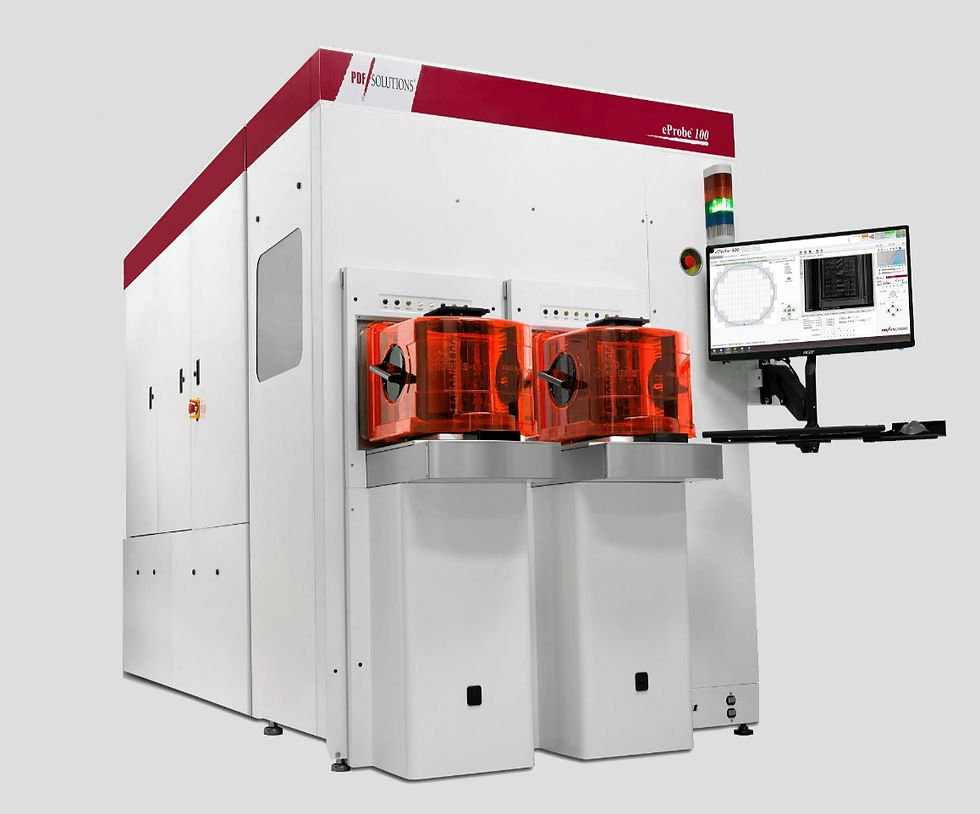
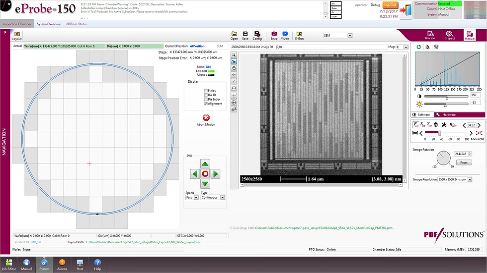
We have been working on a custom scanning electron microscope (SEM) that performs wafer metrology at various points during the manufacturing process to ensure nondestructive inline electrical characterization and process control. Our new system includes both the optical microscope, which uses images from a high-resolution camera, and the SEM, which produces an SEM image. One key innovation that differentiates our system from competing systems is that users can analyze our images in real time instead of offline. For this real-time analysis to work properly, we need extremely fast scanning rates that can produce high-resolution images and measurements with nanometer precision. Our team knew that LabVIEW system design software was the best tool for these enormous control challenges. We also knew we would need help from the best LabVIEW software architects in the industry at JKI.
Rapidly Acquiring an Image to Validate Our Wafer Metrology Process
When we brought JKI into this project, we were working on our system prototype and wanted help acquiring high-resolution images with the SEM at extremely fast acquisition rates. In less than four months, JKI helped us accomplish acquisition rates of 250 MHz per pixel using a FlexRIO board and software developed using the LabVIEW FPGA Module. By using LabVIEW for this part of the process, the PDF/JKI team could easily integrate third-party FPGA IP and implement FPGA logic in a fraction of the time compared to other platforms.
Alignment and Autofocus on the Nanometer Scale
Each time a wafer is brought in for inspection, we need to precisely measure the orientation of the wafer so we can identify features on the nanometer scale. We call this process of finding the offset and angle of each wafer alignment. When a new type of wafer is available, we must perform alignment on the first wafer manually to create an automated alignment file. The PDF/JKI team developed a thorough manual alignment process that goes through several iterations using the SEM and optical microscope. When the alignment is perfect, the system creates an automated alignment file for future use. The alignment file relies heavily on image processing to identify known features at several locations on the wafer, and then uses those positions to calculate alignment values.
Focus quality is another important aspect of imaging with the SEM. We need properly focused images to use them effectively. Moreover, the focus must adjust dynamically because the various inspection areas on the wafer are not flat when analyzed at a nanometer scale. The PDF/JKI team put tremendous effort into creating a robust autofocus algorithm that can operate reliably under adverse imaging conditions (such as high noise and low contrast), and with a high degree of accuracy, for both the SEM and optical microscopes.

Putting It All Together
While LabVIEW delivered the control for the components necessary to perform wafer inspection, a member of our staff used a C# application called the Peer Tool Orchestrator (PTO) to develop the front end of the system. We used JKI to develop an interface that would connect the front end of our system to the back end.
On the back end, LabVIEW controls most of the components that perform wafer inspection, including: controlling the x and y axis for the stage, sampling and driving various I/O points for the electron gun and the column, controlling the load port and equipment front end module, and overseeing the vacuum and interlocking components. LabVIEW also directs and manages the acquisition of both the SEM and optical images. JKI contributed to the software architecture design and the development of various high-level software components that coordinate the low-level hardware functionality, including data acquisition and image manipulation. We needed this low-level functionality to perform wafer alignment and for the overall inspection to successfully take place.
We knew the integration between LabVIEW and PTO would be complex. We provided little guidance to JKI regarding how to achieve the integration. Despite this, and though no one at JKI had faced this kind of challenge before, they hit the ground running. Their team developed the entire application using the JKI Rapid Application Framework for LabVIEW (RAFL) and then built it into a .NET interoperability assembly that can be called by PTO.

Future Development Plans
To advance and fine tune our SEM, we needed a better understanding of how the system is used in the field. We shipped the tool to two customers and asked JKI to send a member of their team to work with each customer on-site. This on-site collaboration was an invaluable step and led to many ideas for ways we can further improve our algorithms to create a more robust and efficient tool.
We have worked with JKI for the past two years. As we continue to advance our SEM system, we anticipate that we will continue our partnership with them. We value our relationship with JKI because every time we face a challenge, we know we can count on their highly skilled team to work collaboratively and solve even the toughest problems. JKI has helped us accelerate our R&D, which has been critical to the successful development of our SEM tool.
Original Authors: Yoram Schwarz, PDF Solutions
Edited by Cyth Systems


